In this article, I will write about DRAM timings. Since a DRAM plays the important role in an operation of the Zen architecture, so it is necessary DRAM tuning when you want to extract better performance of Ryzen. DRAM tuning mainly focuses on the memory frequency and DRAM timings (memory latency). And in Zen2, the optimal memory clock is already determined (3733 MHz or 3800 MHz), so it is important to tune DRAM timings. For better tuning DRAM timings, you should know what it is to some extent. So, I will introduce some of the knowledge about DRAM timings and write down the standards of setting them which I follow, in this article.
今回は,DRAMタイミングについて整理します.Zenアーキテクチャの挙動においてはDRAMが重要な役割を果たすため( https://ocod.home.blog/2019/12/08/why-tuning-ddr4-is-important-for-ryzen/ ),Ryzenの性能をより引き出すためにはDRAMのチューニングを行うことが必要です.DRAMのチューニングは主にメモリクロックとDRAMタイミング(メモリレイテンシ)を対象にしますが,Zen2においては最適なメモリクロックが決まっているため(3733 MHzまたは3800 MHz),DRAMタイミングのチューニングが重要になります.DRAMタイミングのより良いチューニングのためには,それがどのようなものなのかをある程度知っておくのが良いと考えます.そこで,ここではDRAMタイミングにかかわる知識の一部を紹介しつつ,私が個人的に従っている設定基準を記したいと思います.
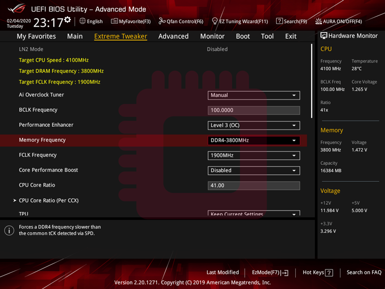
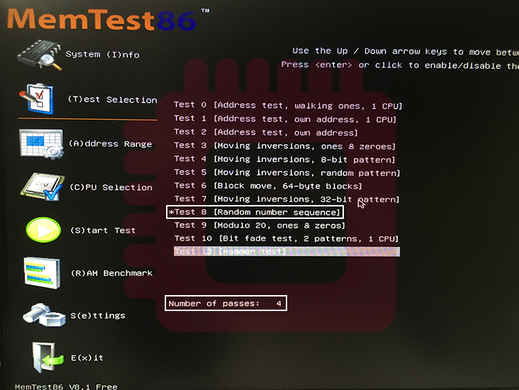
DRAM timings have the primary timings, the secondary timings, the tertiary timings. The range of tuning is often as far as the secondary timings (DRAM Calculator for Ryzen also cover as far as the secondary timings). Therefore, this article targets the primary timings and the secondary timings.
DRAMタイミングには,ファーストタイミング(プライマリタイミング),セカンドタイミング,サードタイミングがあります.DRAMタイミングのチューニングにおいては,セカンドタイミングまでを対象とすることが多いです(DRAM Calculator for Ryzenでも,対象となっているのはセカンドタイミングまでです).したがって,この記事ではセカンドタイミングまでを対象とします.
Knowledge about Operation of SDRAM for Understanding the Primary Timings
The primary timings consists of tRCD, tRP, tRAS, including tCL (CAS latency) which is the most important DRAM timing (and CR is often included). I will write here the outline of 1st timings with introducing the basic operation of DRAM, especially SDRAM including DDR4.
ファーストタイミングには最も重要なDRAMタイミングであるtCL(CASレイテンシ)をはじめ,tRCD,tRP,tRASから成ります(しばしば,CRが含まれることがあります).ここでは,DRAM,特にDDR4を含むSDRAMの基本的な挙動と合わせて,ファーストタイミングの概略を示します.
SDRAM (Synchronous Dynamic Random Access Memory) operates based on clock signals and has the function that synchronizes with the clock of a memory controller (on a CPU) or system buses (transmission paths connecting the chipset and the CPU), and so on. DDR SDRAM (Double Data Rate SDRAM) including DDR4 achieve twice bandwidth per clock compared to SDR SDRAM (Single Data Rate SDRAM, which sends or receives data only at the rising edges of the clock), due to that a CPU distribute read/write processing to two or more memory banks, and each memory banks send or receive data at two timings, the rising edges and the falling edges of a clock. Also, the next command can be issued without waiting for completing the processing by the previous command (for example, a pre command (described later) can be issued before all memory banks have completed reading the data). In addition, in an operation of DRAM, when determine a cell to be read/written, a row is determined first and a column determined second, and there is the function called burst mode which if once the column is determine, the next column is determined automatically for next read/written, and which can save operation time by omitting command to determine the second and subsequent column.
SDRAM(Synchronous Dynamic Random Access Memory)は,クロック信号に基づき動作し,(CPU上の)メモリコントローラーやシステムバス(チップセットとCPUをつなぐ伝送路)等のクロックと同期する仕組みを持っています.DDR4等のDDR SDRAM(Double Data Rate SDRAM)は,CPUが2つ以上のメモリバンクに読み書きの処理を振り分け,それぞれのメモリバンクがクロックの立ち上がりと立ち下がりの2つのタイミングでデータを送受信することで,SDR SDRAM(Single Data Rate SDRAM,これのデータ送信はクロックの立ち上がりのみで行われる)に対し,クロック当たり2倍の帯域を実現しています.また,DDR SDRAMは,以前の命令の処理の完了を待たずに次の命令を発行することができます(すべてのメモリバンクがデータの読み取りを完了する前にpreコマンド(後述)を発行できる,等).さらにDRAMの動作では,読み書きの対象となるセルの指定に当たり,まず行を指定し次に列を指定しますが,一度特定の列が指定されれば自動的に次の列が次の読み書きの対象となるバーストモードという機能を備えており,2回目以降の列指定の命令を省くことで動作時間の短縮に貢献します.
To understand some DRAM timings, you need to know some of the basic commands in DRAM operation.
いくつかのメモリタイミングを理解するために,DRAMの動作における基本的なコマンドのいくつかを知る必要があります.
- CS (chip select): It determines which memory chip is being accessed.
- act (activate): It determines a bank address and a row address.
- read/write: It determines a column address, and read/write data. It also include auto precharge individual columns.
- pre (precharge): It closes the row (thus the row has remained open til fetch a precharge command), terminates all operation, and returns the memory chip to the standby state.
- ref (refresh): The capacitors used for DRAM are volatile (they leaks electric charge unless written), so data will be lost if left untouched. To prevent this, it is necessary to periodically rewrite (refresh) the precharged memory chip.
- CS(chip select):どのメモリチップにアクセスするかを決定します.
- act(activate):バンクアドレスと列アドレスを決定します.
- read/write:列アドレスを決定し,データを読み書きします.また,個々の列を自動プリチャージします.
- pre(precharge):行を閉じて(つまり,preコマンドが受け取られるまで行が開いたままになります)すべての操作を終了し,メモリチップをスタンバイ状態に戻します.
- ref(refresh):メモリに用いられるコンデンサは揮発性のため(書き込みをしない限り電荷がリークされる)そのままではデータが損失します.これを防ぐため,プリチャージされたメモリチップに定期的に再書き込みを行う(リフレッシュを行う)必要があります.

Meaning of the Primary Timings
The primary timings are the most basic and important one of DRAM timings. Since there are few kinds of primary timings, the basic tuning method is to reduce the value one by one while balancing with the DRAM voltage based on the XMP of the DRAM.
プライマリタイミングは,DRAMタイミングのうち最も基本的かつ重要なものです.プライマリタイミングは数も少ないため,DRAMのXMPを基準に,DRAM電圧とのバランスをとりながら値を1ずつ削減していくことが基本的な調整方法になります.
- tCL or tCAS (Column Address Strobe Latency): This means the number of clocks from when a column is selected by read/write command to when start read/written data. There are three types of read/write transaction of DRAM corresponding to status of the bank (page): Page-Hit Access (when the bank targeted to read/written is already open, and an act command isn’t required); Page-Empty Access (when the bank targeted to read/written is closed, so an act command is required); Page-Miss Access (when the wrong row is being opened so it is necessary to close the row opened currently and open a different row, thus it is necessary not only act command but also pre command before the act command). And tCL is the latency intervene in all of them, thus, tCL greatly affects the performance of DRAM. Therefore, it is important to reduce tCL preferentially.
- tRAS (Raw Address Strobe Latency): This means the minimum number of clocks required from when selecting a row by an act command to when issuing a pre command. The target row remains opened during column selection and data reading/writing, so the range of tRAS is till a precharge command.
- tRCD (Row Address to Column Address Delay): This means the minimum number of clocks required from when selecting a row by an act command to when issue a read/write command. There are two kinds of tRCDs: tRCDWR is tRCD which is required when a write command is issued; tRCDRD is required when a read command is issued.
- tRP (Row Precharge Time): This means the minimum number of clocks required to complete a precharging.
- CR (Command Rate): This means the number of consecutive clocks required when a memory controller sends commands to a memory bank. The CR is indicated as 1T or 2T (often 1N or 2N), each means one clock and two clocks. If the CR is 1T, each of the commands are sent only once to the memory bank which takes one clock (therefore, one clock delay occurs), and if 2T, each of the commands are sent twice which takes one clock (therefore, two clocks delay occurs). Since the CR is delay about each of the commands, it significantly influence the performance of DRAM. So you should set 1T (1N) preferentially.
- tCLまたはtCAS(Column Address Strobe Latency):これは,read/writeコマンドにより列が選択されてからデータの読み書きが開始されるまでのクロック数を意味します.DRAMの読み書きには,バンク(ページ)の状況に応じて,ページヒットアクセス(バンクが既に開いている状態での読み書きで,actコマンドは不要),ページエンプティアクセス(バンクが閉じている状態での読み書きで,actコマンドが必要),ページミスアクセス(誤った行を開いているため,現在開いている行を閉じて異なる行を開く必要がある状態での読み書きで,actコマンドに加えて,その前にpreコマンドが必要)の3種類が存在します.tCLはそのすべてに介在する遅延であり,DRAMの性能に多大な影響を及ぼします.したがって,他のタイミングに優先してtCLを減らすことが重要になります.
- tRAS(Raw Address Strobe Latency):これは,actコマンドによる行の選択からpreコマンドの発行までに必要な最小クロック数を意味します.列の選択やデータの読み書きの間,対象となっている行は開いたままなので,tRASの範囲はプリチャージまでということになります.
- tRCD(Row Address to Column Address Delay):これは,actコマンドによる行の選択からread/writeコマンドの発行までに必要な最小クロック数を意味します.tRCDには,writeコマンドが発行された時に要求されるtRCDWR,readコマンドが発行された時に要求されるtRCDRD,の2種類があります.
- tRP(Row Precharge Time):これは,プリチャージが完了するまでに必要な最小クロック数を意味します.
- CR(Command Rate):これは,メモリコントローラがメモリバンクにコマンドを送る際に必要な連続したクロック数を意味します.CRは,1Tや2T(しばしば,1Nや2N)と表記されますが,これはそれぞれ1クロックと2クロックを意味します.CRが1Tの場合,各コマンドは1クロック分かけてメモリバンクに1度だけ送られ(したがって,1クロックの遅延が生じます),2Tの場合,各コマンドは1クロック分かけて2度送られます(したがって,2クロックの遅延が生じます).CRは各コマンドにかかる遅延であるため,メモリの性能に大きな影響を及ぼします.したがって,優先的に1T(1N)で設定します.
About the True Latency
The latency related to the commands in SDRAM (DRAM timings) is indicated in clock units, via the character of operation of SDRAM that synchronize with clock signals. For example, tCL 2 means that the latency between opening a column and reading/writing data is 2 clocks. The tCL can also be expressed in actual time, which is called true latency and is calculated as follows.
SDRAMにおけるコマンドにかかわる遅延(メモリタイミング)は,クロック信号に同期して動作する特徴から,クロック単位で示されます.例えば,tCL 2は,列の開放からデータの読み書きまでの遅延が2クロック分であることを意味します.tCLは実際の時間で表記することもでき,それは実レイテンシと呼ばれ以下のように計算します.
True Latency = tCL / memory frequency
When comparing multiple DRAMs, if the memory frequencies are different, the required time at Column Address Strobe indicated by the number of clocks will be different. If you want to compare the performance of DRAMs with different memory frequencies and DRAM timings, for this reason, it is necessary to refer to True Latency. The higher value of the memory frequency and the smaller value of DRAM timing means the better DRAM respect of performance, and therefore, the DRAM which have the smaller True Latency is the better one.
複数のDRAMを比較する際,そのメモリクロックが異なるとクロック数で表記されているColumn Address Strobeで要求される時間が異なってきます.それぞれ異なるメモリクロックとメモリタイミングをもつDRAMの性能を比較する際には,こうした理由から,実レイテンシ参照する必要が出てきます.メモリクロックの数値は大きくメモリタイミングの数値は小さい方が高性能のDRAMということになり,したがって小さい実レイテンシを持つDRAMは良いということになります.
For Zen2, it has been recommended that you set memory frequency 3733 MHz or 3800 MHz, and it is ok to overclock a DRAM which works 3200 MHz or to downclock a DRAM which works 4000 MHz. This True Latency can be helpful when choosing a DRAM to use with a Zen 2 processor. For example, in the case of (I) F4-3200C14-8gGFX (3200 MHz, CL14), (II) F4-3600C15-8gGTZ (3600 MHz, CL15) and (III) F4-4000C17-8GTZR (4000 MHz, CL17), the each actual latency is (I) 8.75 ns, (II) 8.33 ns, and (III) 8.5 ns, so the performance when operating at XMP is (II) > (III) > (I).
Zen2では3733 MHzまたは3800 MHzのメモリクロックが推奨されていますが,3200 MHzのメモリをオーバークロックしたり,4000 MHzのメモリをダウンクロックして使っても問題はありません.Zen 2プロセッサで使うメモリの選択の際に,この実レイテンシは参考になります.例えば,(I) F4-3200C14-8gGFX(3200 MHz, CL 14)と (II) F4-3600C15-8gGTZ(3600 MHz, CL 15)と (III) F4-4000C17-8GTZR(4000 MHz, CL 17)の場合,実レイテンシは(I) 8.75 ns,(II) 8.33 ns,(III) 8.5 nsとなり,XMPで動作した場合の性能は(II) > (III) > (I)です.
Meaning of the Secondary Timings and Standards for Setting Them
- tRC (Row Cycle Time): This means the minimum number of clocks from when opening a row to when completing precharging (row cycle). tRC = tRP + tRAS.
- tRRD (RAS to RAS Delay): This is the number of clocks required between two issuance of the RAS signal (which is enabled between the act command and the pre command). There are two kinds of tRRDs: tRRDS means tRRD among different memory bank groups; tRRDL means among the same memory bank groups. The values I often use are: tRRDS -> 4; tRRDL -> 6.
- tFAW (Four Activate Window): DRAM can be activated up to four memory banks (and rows) per memory rank, and tFAW means the time between when four memory banks are opened to when the next memory bank can be opened. tFAW = 4 * tRRDS.
- tWTR (Write to Read Delay): This means the number of clocks required after a write command was completed successfully before a read command can be issued. There are two kinds of tWTRs: tWTRS means tWTR among different memory bank groups; tWTRL means among the same memory bank groups. The values I often use are: tWTRS -> 6; tWTRL -> 8.
- tWR (Write Recovery Time): This means the number of clocks required after a write command was completed successfully before a pre command is issued. The value I often use is: tWR -> 12.
- tRFC (Refresh Cycle Time): This means the number of clocks required from when a ref command is issued to when the next act command can be issued. tRFC = n * tRC, n = 6 or 7. One of the strengths of the Samsung B-Die chip is that it can significantly reduce tRFC, so it is best to target less than 300 when tuning the DRAM in which it is used. (And tRFC has two other variations, but in Ryzen, they aren’t used: tRFC2 = tRFC / 1.346 (at double frequency mode); tRFC4 = tRFC2 / 1.625 (at quad frequency mode).)
- tCWL (CAS Write Latency): It is the number of clocks required from when an activation of the column of DRAM to when the execution of the write command, and it is de facto tCL. tCWL = tCL.
- tRTP (Read to Precharge Delay): This means the number of clocks required from when issuance of the read command to when issurance the pre command in the same memory rank. tRTP = tWR / 2.
- tCKE (Clock Enable Time): This means the number of clocks required to issue a CKE signal. All commands of DRAM operations are fetched only when the CKE signal is high (that is, commands are not read when the CKE signal is low). Therefore, when PowerDownMode (function to make the CKE signal low) is off, the value of tCKE has no effect on the DRAM operation because the CKE signal doesn’t become low.
- tRDRD (Read to Read Delay): This means the number of clocks required from when a read command is issued to when the next read command can be issued. There are four kinds of tRDRDs: tRDRDSc means tRDRD among different memory bank groups; tRDRDScL means among the same memory bank groups; tRDRDSd means among different memory ranks; tRDRDDd means among different DRAMs. The values I often use are: tRDRDSc -> 1; tRDRDScL -> 4; tRDRDSd -> 4; tRDRDDd -> 4.
- tWRWR (Write to Write Delay): This means the number of clocks required from when a write command is issued to when the next write command can be issued. There are four kinds of tWRWRs: tWRWRSc means tWRWR among different memory bank groups; tWRWRScL means among the same memory bank groups; tWRWRSd means among different memory ranks; tWRWRDd means among different DRAMs. The values I often use are: tWRWRSc -> 1; tWRWRScL -> 4; tWRWRSd -> 6; tWRWRDd -> 6.
- tRDWR (Read Write Command Spacing): This means the number of clocks required from when a read command is issued to when the next write command can be issued in the same memory rank. The value I often use is: tRDWR -> 8.
- tWRRD (Write Read Command Spacing): This means the number of clocks required from when a read command is issued to when the next write command can be issued in the same memory rank. The value I often use is: tWRRD -> 2.
- tRC(Row Cycle Time):これは,actコマンドによって行が開いてからprechargeが完了するまで(行サイクル)の最小クロック数を意味します.tRC = tRP + tRAS.
- tRRD(RAS to RAS Delay):これは,2つの(actコマンドからpreコマンドの間有効になっている)RAS信号の発行に必要な間隔をクロック数で表したものです.tRRDには,異なるメモリバンクグループにおけるtRRDを意味するtRRDSと,同じメモリバンクグループにおけるtRRDLの2種類があります.著者がよく使う値は,tRRDS -> 4; tRRDL -> 6.
- tFAW(Four Activate Window):DRAMでは1つのメモリランクにつき最大4つのメモリバンク(と行)をアクティベートできますが,tFAWは4つのメモリバンクが開かれた後,次のメモリバンクを開くことができるようになるまでの時間を意味します.tFAW = 4 * tRRDS.
- tWTR(Write to Read Delay):これは,writeコマンドが正常に完了してからreadコマンドを発行できるようになるまでに必要なクロック数を意味します.tWTRには,異なるメモリバンクグループにおけるtWTRを意味するtWTRSと,同じメモリバンクグループにおけるtWTRLの2種類があります.著者がよく使う値は,tWTRS -> 6; tWTRL -> 8.
- tWR(Write Recovery Time):これは,writeコマンドが正常に完了してからpreコマンドが発行されるまでに必要なクロック数を意味します.著者がよく使う値は,tWR -> 12.
- tRFC(Refresh Cycle Time):これは,refコマンドが発行されてから次のactコマンドが発行できるようになるまでに必要なクロック数を意味します.tRFC = n * tRC, n = 6 or 7.Samsung B-DieチップはtRFCを大きく削減できることが長所の1つなので,それが使用されているDRAMをチューニングする場合,300以下にすることを目標にするといいでしょう.(また,tRFCには他に2種類のバリエーションが存在しますが,Ryzenにおいては使用されません.tRFC2 = tRFC / 1.346(double frequency mode); tRFC4 = tRFC2 / 1.625 (quad frequency mode))
- tCWL(CAS Write Latency):DRAMの列をアクティベートしてからwriteコマンドを実行するまでに必要となるクロック数で,事実上のtCLです.tCWL = tCL.
- tRTP(Read to Precharge Delay): これは,同じメモリランクにおける,readコマンドの発行からpreコマンドの発行までに必要なクロック数を意味します.tRTP = tWR / 2.
- tCKE(Clock Enable Time):これは,CKE信号の発行に必要なクロック数のことを意味します.DRAMの動作にかかわるすべてのコマンドは,CKE信号がハイの場合にのみフェッチされます(つまり,CKE信号がローの状態はコマンドが読み取られません).したがって,PowerDownMode(CKE信号をローにする機能)をoffにしている場合,CKE信号がローにならないため,tCKEの値はDRAMの動作に影響力を持ちません.
- tRDRD(Read to Read Delay):これは,readコマンドが発行されてから次のreadコマンドが発行できるようになるまでに必要なクロック数を意味します.tRDRDには,異なるメモリバンクグループにおけるtRDRDを意味するtRDRDSc,同じメモリバンクグループにおけるtRDRDScL,異なるメモリランクにおけるtRDRDSd,異なるDRAMにおけるtRDRDDd,の4種類があります.著者がよく使う値は,tRDRDSc -> 1; tRDRDScL -> 4; tRDRDSd -> 4; tRDRDDd -> 4.
- tWRWR(Write to Write Delay):これは,writeコマンドが発行されてから次のwriteコマンドが発行できるようになるまでに必要なクロック数を意味します.tWRWRには,異なるメモリバンクグループにおけるtWRWRを意味するtWRWRSc,同じメモリバンクグループにおけるtWRWRScL,異なるメモリランクにおけるtWRWRSd,異なるDRAMにおけるtWRWRDd,の4種類があります.著者がよく使う値は,tWRWRSc -> 1; tWRWRScL -> 4; tWRWRSd -> 6; tWRWRDd -> 6.
- tRDWR(Read Write Command Spacing):これは,同じメモリランクにおいて,readコマンドが発行されてから次のwriteコマンドが発行できるようになるまでに必要なクロック数を意味します.著者がよく使う値は,tRDWR -> 8.
- tWRRD(Write Read Command Spacing):これは,同じメモリランクにおいて,writeコマンドが発行されてから次のreadコマンドが発行できるようになるまでに必要なクロック数を意味します.著者がよく使う値は,tWRRD -> 2.