

If you want to overclock DRAMs or reduce DRAM timings from XMP further, it is known that you can use Ryzen DRAM Calculator released by 1usmus. This calculates some values very easily, including detailed items. However, it is largely depends on your individual environment (system configuration) that those values are appropriate or not. Therefore, you just only enter values calculated by the calculator, you often get failure to start your system or instability on your daily operation. Thus, the calculator only provides a draft, and based on that, you should specify the optimal values of each item according to your own environment. It can be said that that is appropriate usage of Ryzen DRAM Calculator.
XMPからさらにDRAMをオーバークロックしたりDRAMタイミングを減少させる場合,1usmus氏によってリリースされているRyzen DRAM Calculatorを利用できることが知られています.これは細かな項目を含めて非常に簡単にいくつかの値を算出してくれますが,これらの項目の値が適切であるか否かは,個別の環境(システム構成)に大きく依存しています.したがって,ただ計算機から算出された値を入力しただけでは,システムの起動に失敗したり日常動作が不安定になることがしばしばあります.つまり,計算機はあくまでたたき台を提示するものであって,それを元に自分の個別の環境に合わせて各項目の適切な値を特定していく必要があります.それが,Ryzen DRAM Calculatorの適切な使用法だと言えます.
On this article, I will instruction a method for stable DRAM tuning, especially finding the optimal values of termination resistances, on Ryzen. Termination resistances are used for impedance matching that are ratio of current to voltage. If there are no termination resistances or inadequate termination resistances, impedances among the side of signal output, the side of signal input, and of the transmission passes (called “characteristic impedance”) become inconsistent. In this case, the transmitted signal is reflected at the end of the circuit, and the power which transmits the signal is attenuated (similar to a water wave bouncing off a wall). That is recognized that noises which degrade the signal waveform, and this can be fatal in the exchange of high-frequency signals, causing read/write errors. Because of that, tuning termination resistances to reduce noise is important when you overclock DRAMs.
今回は,Ryzenにおける安定したメモリの調整方法,特に,適切な終端抵抗の値を調べる方法を説明します.終端抵抗は,インピーダンス(電流と電圧の比)を整合させるためのものです.終端抵抗がない,あるいは不適切な終端抵抗になっている場合,信号の発信側と受信側,そして伝送路のインピーダンス(これを特性インピーダンスといいます)が不整合になります.この場合,送信された信号は回路の末端で反射し,信号を送信する電力が減衰します(壁で跳ね返る水の波のようなものです).それは信号波形を劣化させるノイズとして認識され,これは高周波信号のやりとりにおいては致命的となって読み書きのエラーを生じさせます.このため,ノイズを抑えるための終端抵抗の調整は,DRAMのオーバークロックにおいて重要になります.
Things to Prepare
memtest86 (bootable from an USB stick)
DRAM Calculator for Ryzen v1.7.0 by 1usmus (latest version as of February 5th, 2020)
https://www.techpowerup.com/download/ryzen-dram-calculator/
*Thank you, 1usmus!
Equipment Used for the Tests for This Article
- Ryzen 9 3950X (core clock 4100 MHz)
- F4-3600C14Q-32GTZN (use only 2 DRAMs)
- X570 ROG Crosshair VIII HERO Wi-Fi (AGESA 1.0.0.4)
STEP1. Set Some Basic Items
Set target values, memory frequency, DRAM timings, DRAM voltage, CPU SoC voltage, VTT DDR voltage, and BGS (BankGroupSwap), for daily-use from UEFI.
UEFIから,DRAMクロック,DRAMタイミング,DRAM電圧,CPU SoC電圧,VTT DDR電圧,BGS(BankGroupSwap)を,常用の目標値に設定します.
memory frequency… For Zen2, the optimal memory frequency is 3733 MHz or 3800 MHz (https://ocod.home.blog/2019/12/08/why-tuning-ddr4-is-important-for-ryzen/).
メモリクロック… Zen2の場合,最適なメモリクロックは3733 MHzまたは3800 MHzです( https://ocod.home.blog/2019/12/08/why-tuning-ddr4-is-important-for-ryzen/ ).
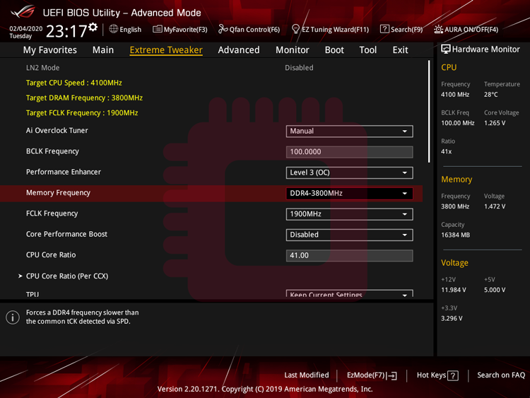
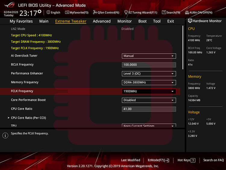
If fClk does not synchronize automatically with mClk, you should set manually fClk to 1867 MHz or 1900 MHz from UEFI.
fClkが自動でmClkと自動的に同期しない場合,UEFIから手動で1867 MHzまたは1900 MHzに設定します.
DRAM timings… ( https://ocod.home.blog/2020/02/29/what-are-dram-timings-some-knowledge-about-operation-of-sdram-and-a-brief-memorandum-about-dram-timings/ )
DRAMタイミング… ( https://ocod.home.blog/2020/02/29/what-are-dram-timings-some-knowledge-about-operation-of-sdram-and-a-brief-memorandum-about-dram-timings/ )
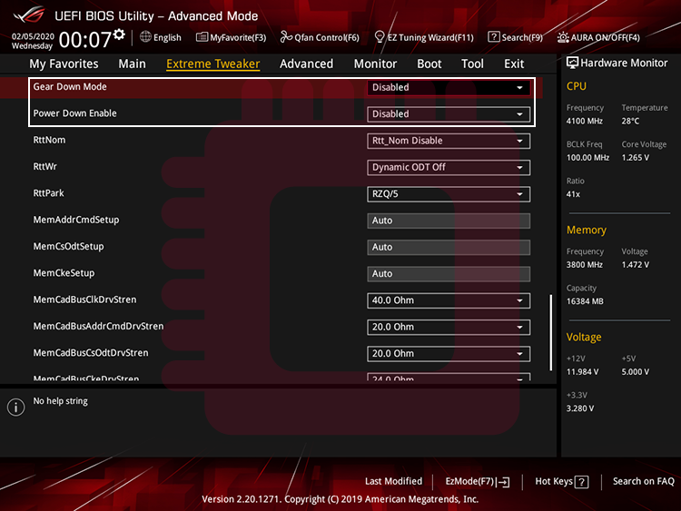
If Gear Down Mode is enabled, you cannot set an odd value of tCL, so turn it off. And Power Down Mode is the function that puts the DRAM in sleep mode when your system is inactive. If you want to use the full performance of the DRAM, turn it off.
Gear Down Modeが有効になっていると奇数の値のtCLを設定することができないので,これをオフにします.また,Power Down Modeは非アクティブ時にDRAMを休止状態にする機能ですが,DRAMの性能をフルで使いたい場合,これをオフにします.
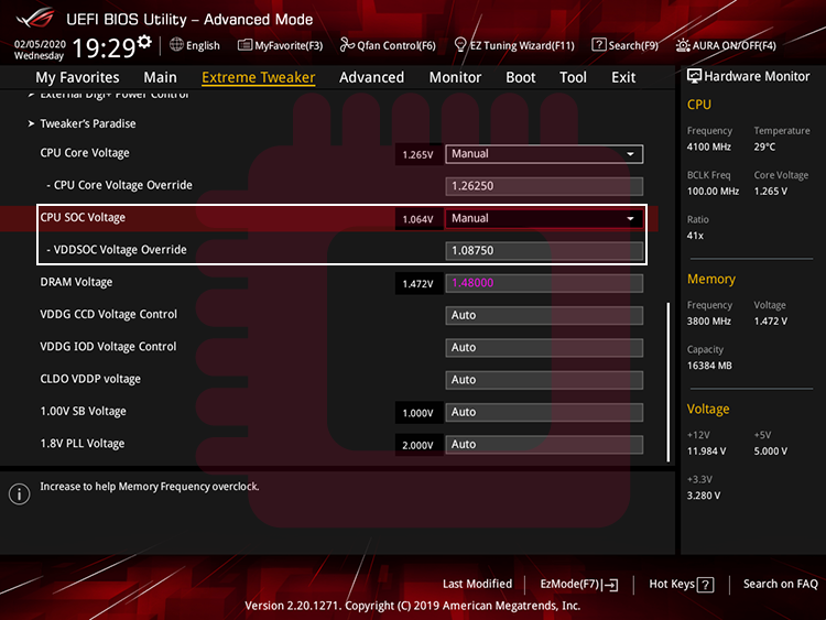
DRAM voltage… If you use Samsung B-Die memories, up to 1.5 V or slightly higher for daily-use.
DRAM電圧… Samsung B-dieを使用する場合,常用では1.5 Vかそれよりわずかに高い値を上限とします.
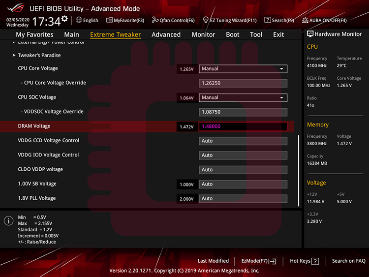
VTT DDR voltage… It means termination voltage. If impedances among the side of signal output, the side of signal input, and a characteristic impedance are matched, termination voltage will be half of DRAM voltage ( = voltage applied a side of signal output). That is because a termination voltage is affected by two resistances, one is the resistance applied to the side of signal output and the other is the termination resistance. When impedances are matched, resistance applied to the side of signal output and termination resistance will have same value generally, so the optimal termination voltage become half of DRAM voltage. As I’ll do below, our purpose in this article is find optimal termination resistance. When you want to find optimal value of a variable, you should fix values of another variables which effect that variable. So you should set VTT DDR voltage half of DRAM Voltage.
VTT DDR電圧… これは終端電圧を意味します.信号出力側,信号入力側,特性インピーダンスのインピーダンスが一致している場合,終端電圧はDRAM電圧(=信号出力側の電圧)の半分になります.これは終端電圧が2つの抵抗の影響を受けるためです.1つは信号出力側の抵抗で,もう1つは終端抵抗です.インピーダンスが一致すると,信号出力側に適用される抵抗と終端抵抗は,一般的に同じ値になるため,最適な終端電圧はDRAM電圧の半分になります.以下で行うように,ここでの目的は最適な終端抵抗を見つけることです.ある変数の最適値を見つけたいときには,その変数に影響を与える他の変数の値を固定する必要があります.したがって,DRAM電圧の半分のVTT DDRを設定します.

CPU SoC voltage… It is applied to memory controller on the CPU. Up to 1.1 V or slightly higher for daily-use.
CPU SoC電圧… これはCPUのメモリコントローラーに適用されます.常用では1.1 Vかそれよりわずかに高い値を上限とします.
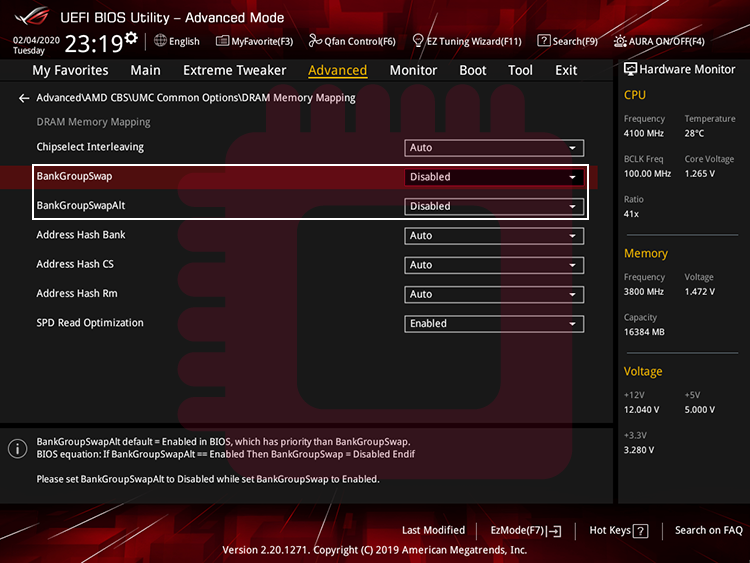
BGS… BGS is a function to assign applications to physical areas of memory modules. When this is turned on, it brings benefit at running synthetic test apps and disadvantage at running game apps (https://community.amd.com/community/gaming/blog/2017/07/14/memory-oc-showdown-frequency-vs-memory-timings). If you value practicality, I think it is better to turn BankGroupSwap and BankGroupSwapAlt off.
BGS… BGSは,メモリモジュールの物理領域にアプリケーションを割り当てる機能です.これをオンにすると,総合テストアプリの実行における利益をもたらす一方で,ゲームアプリの実行におけるデメリットがもたらされます(https://community.amd.com/community/gaming/blog/2017/07/14/memory-oc-showdown-frequency-vs-memory-timings).実用性を重視する場合,BankGroupSwapとBankGroupSwapAltをオフにする方が良いと考えます.
STEP2. Set Values of CAD_Bus Drive Strength
The appropriate values for impedance matching depends on the combination of a motherboard, a memory, a SoC (in a CPU), and a value of memory clock, so you have to test each values one by one.
インピーダンスマッチングの適切な値は,マザーボード,メモリ,(CPU内の)SoC,メモリクロックの組み合わせに依存するため,しらみつぶしにテストしていくしかありません.
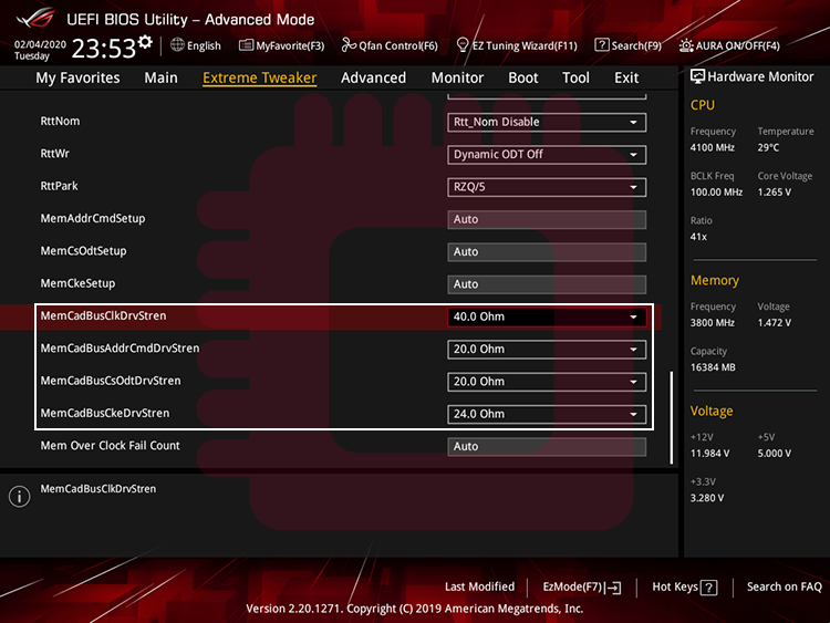
CAD_Bus (Command/Address/Data_Bus) Drive Strength… It means resistances which is applied to pins on a DRAM. Enter provisionally the values calculated by the DRAM Calculator. The optimal values of CAD_Bus Drive Strength depend on the circumstance composed by your PC parts, so you should adjust that later.
CAD_Bus(Command/Address/Data_Bus)Drive Strength… これはDRAM上のピンにかかる抵抗を意味します.DRAM Calculatorで計算された値を暫定的に入力します.適切なCAD_Bus Drive Strengthの値はPCパーツによって構成される状況に依存しているため,後で調整する必要があります.
- ClkDrvStren (Clock Drive Strength)… It means a resistance of MEMCLK (Memory Clock) pin.
- AddrCmdDrvStren (Address/Command Drive Strength)… It means resistances of each pins; Address, RAS# (Row Address Strobe), CAS# (Column Address Strobe), WE# (Write Enable), Bank, and Parity.
- CsOdtDrvStren… (Chip Select/On-Die Termination Drive Strength)… It means resistances of each pins of CS# (Chip Select), and ODT (On-Die Termination).
- CkeDrvStren (Clock Enable Drive Strength)… It means a resistance of CKE (Clock Enable) pin.
- ClkDrvStren (Clock Drive Strength)… MEMCLK(Memory Clock)ピンの抵抗を意味します.
- AddrCmdDrvStren (Address/Command Drive Strength)…Address,RAS#(Row Address Strobe),CAS#(Column Address Strobe),WE#(Write Enable),Bank,Parityの各ピンの抵抗を意味します.
- CsOdtDrvStren… (Chip Select/On-Die Termination Drive Strength)… CS#(Chip Select)及びODT(On-Die Termination)ピンの抵抗を意味します.
- CkeDrvStren (Clock Enable Drive Strength)… CKE(Clock Enable)ピンの抵抗を意味します.

STEP3. Set Values of Termination Resistance (1): Set Values of Rtt
Rtt… It means termination resistance which is applied each dies of DRAM individually, and it depends on the number of ranks of DRAM. Enter the values calculated by the DRAM Calculator.
Rtt… これはDRAMの各ダイに個別に適用される終端抵抗を意味し,DRAMのランクの数に依存します.DRAM Calculatorで計算された値を入力します.
- Rtt_NOM (Nominal On-Die Termination Impedance) & Rtt_PARK (Park On-Die Termination Impedance)…They contribute to prevent signal degradation about dies which is not executing write commands.
- Rtt_WR (Write On-Die Termination Impedance)… It contribute to prevent signal degradation about dies which is executing writing commands.
- Rtt_NOM (Nominal On-Die Termination Impedance) & Rtt_PARK (Park On-Die Termination Impedance)… これらは書き込みコマンドを実行していないダイについての信号の乱れの防止に貢献します.
- Rtt_WR (Write On-Die Termination Impedance)… これは書き込みコマンドを実行しているダイについての信号の乱れの防止に貢献します.


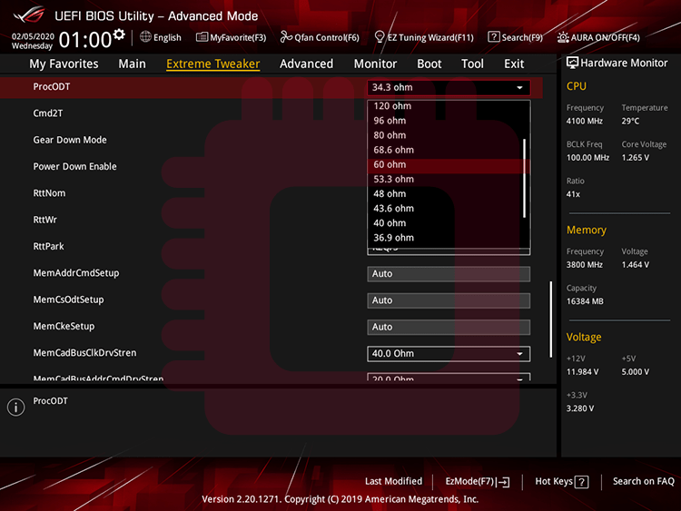
STEP4. Set Values of Termination Resistance (2): Find the Optimal ProcODT
ProcODT (Processor On-Die Termination)… It means termination resistance. We will test each values one by one, and safe line for daily-use is under 60 Ohm.
ProcODT (Processor On-Die Termination)… これは終端抵抗を意味します.ProcODTの値を1つずつ検証します.常用では60 Ω以下が安全です.
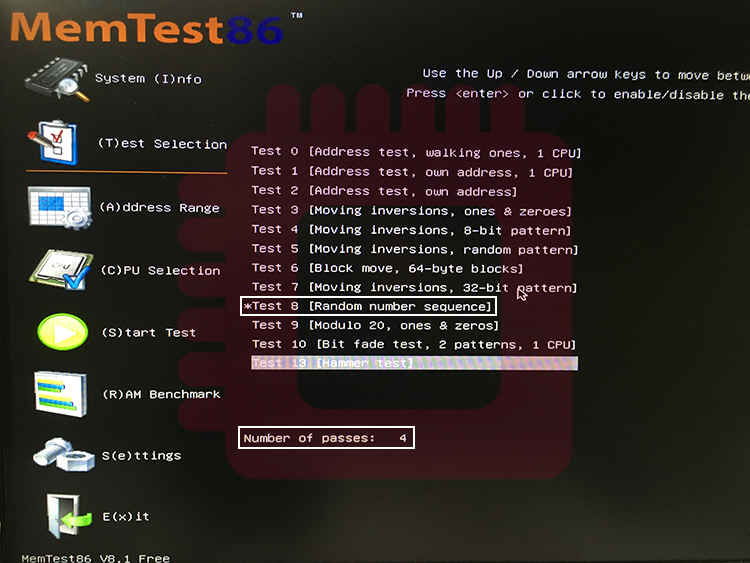
Boot memtest86 and execute only test8, ‘Random Number Sequence,’ for 4 times.
memtest86を起動し,test8「Random Number Sequence」のみを4回実行します.
Run the test for 1 and half minute and record the number of errors for each ProcODT. The one with the fewest number of errors is the optimal ProcODT (it is recommended to list some ProcODTs with fewer number of errors, because memtest86 don’t provide rigid results). If the number of errors is large (such as over 100), the values set in STEP 1 is inappropriate. In that case, you should adjust some values by increasing values of the DRAM timings or the DRAM voltage.
テストを1分30秒実行し,それぞれのProcODTごとのエラー数を記録します.もっともエラー数の少ないものが最適なProcODTになります(テスト結果に誤差が生じる場合があるため,少ないエラー数のProcODTをいくつかリストアップしておくことをおすすめします).エラー数が多い場合(100を超える等),STEP 1で設定した数値は不適切です.DRAMタイミングを緩めたりDRAM電圧を上げる等してください.
If you have no errors, decrease DRAM voltage temporarily to occurring errors to find the adequate value. In that case, restore the DRAM voltage as soon as the optimal values is found.
エラーが生じない場合,DRAM電圧を一時的に下げてエラーを発生させ,最適値を見つけます.最適値が見つかり次第,DRAM電圧を元に戻してください.
STEP5. Find the Optimal Values of CAD_Bus Drive Strength
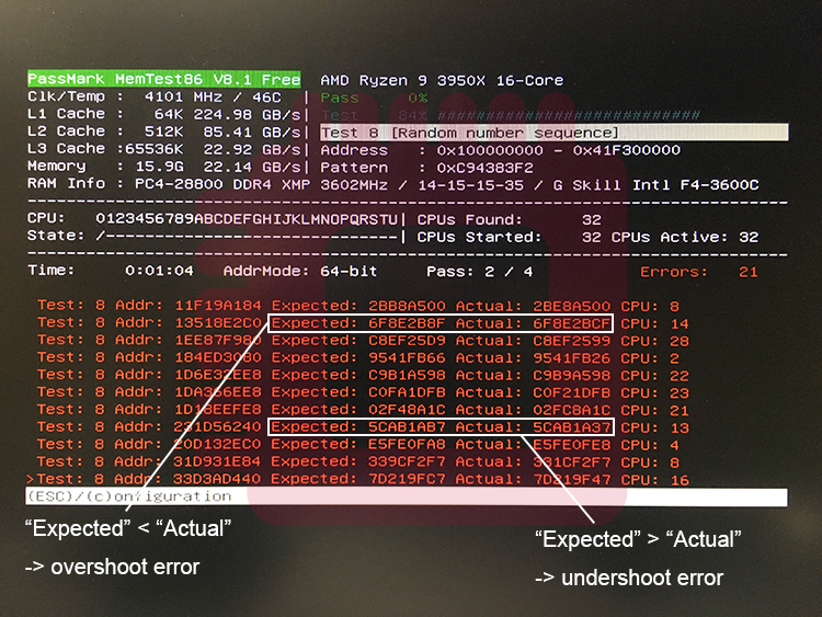
Run test8 of memtest86 again and note the error results (“Expected” and “Actual”) as much as possible. Then, compare the values of “Expected” and “Actual” and records the numbers of results where “Actual” is higher(/lower) than “Expected”. Current CAD_BUS Drive Strength is lower than optimal one when the numbers of result of “‘Expected’ < ‘Actual'” (overshoot errors) was more occur than opposite ones. And current CAD_BUS Drive Strength is higher than optimal one when the numbers of case of “‘Expected’ > ‘Actual'” (undershoot errors) was more occur than opposite ones.
再度memtest86のtest8を実行し,生じたエラーの結果(「Expected」,「 Actual」)を可能な限りメモします.そして,「Expected」と「Actual」の数値を比較し,「Actual」が「Expected」より高い結果の数と低い結果の数を記録します.「Actual」が「Expected」より高い結果が多い(オーバーシュートエラーが多い)場合は今のCAD_Bus Drive Strengthが理想値より低く,「Actual」が「Expected」より低い結果が多い(アンダーシュートエラーが多い)場合は今のCAD_Bus Drive Strengthが理想値より高いことを示しています.
When changing the value of CAD_Bus Drive Strength, increase/decrease the value of all items of CAD_Bus Drive Strength at the same time. If the number of overshoot and undershoot errors is close to the same number, that is the appropriate values of CAD Bus Drive Strength.
CAD_Bus Drive Strengthの値を変更する場合,全てのCAD_Bus Drive Strengthの項目の値を同時に増減させてください.オーバーシュートエラーとアンダーシュートエラーが同数近くなったら,それが適切なCAD_Bus Drive Strengthの値です.
If you have no errors, decrease DRAM voltage temporarily to occurring errors to find the adequate value. In that case, restore the DRAM voltage as soon as the optimal values is found.
エラーが生じない場合,DRAM電圧を一時的に下げてエラーを発生させ,最適値を見つけます.最適値が見つかり次第,DRAM電圧を元に戻してください.
STEP6. Durability Test, and Revising Values of Some Items
If you find the optimal values of ProcODT and CAD Bus Drive Strength, run HCI Mem Test on DRAM Calculator (set default RAM size, task scope 400%, and single task mode). And adjust DRAM timings, DRAM voltage, and CPU SoC voltage until no errors are occurred.
ProcODTとCAD_Bus Drive Strengthの値が決まったら,DRAM CalculatorのHCI Mem Test(RAMサイズはデフォルト,task scopeは400%,single taskモードに設定)を実行します.そして,エラーが0になるまでDRAMタイミングとDRAM電圧,CPU SoC電圧を調整します.

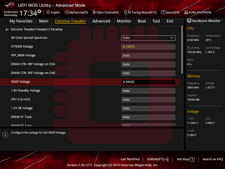
Appendix. Tweaking VDDP Voltage
When some errors occur though you set optimal values of above items, increase the value of VDDP voltage may be effective. VDDP voltage means a voltage which is applied to interface (on SoC) with signals from DDR4. Try to increase the value of VDDP voltage in units of 10 mV or 15 mV from 855 mV up to 950 mV.
上記の各項目について最適値を設定しているにもかかわらずエラーが生じる場合,VDDP電圧を上げると効果があるかもしれません.VDDP電圧はDDR4からの信号との(SoC上の)インターフェースにかかる電圧を意味します.VDDP電圧を855 mV から950 mVにかけて,10 mVか15 mV単位で上げてみてください.
Result in the Test for This Article
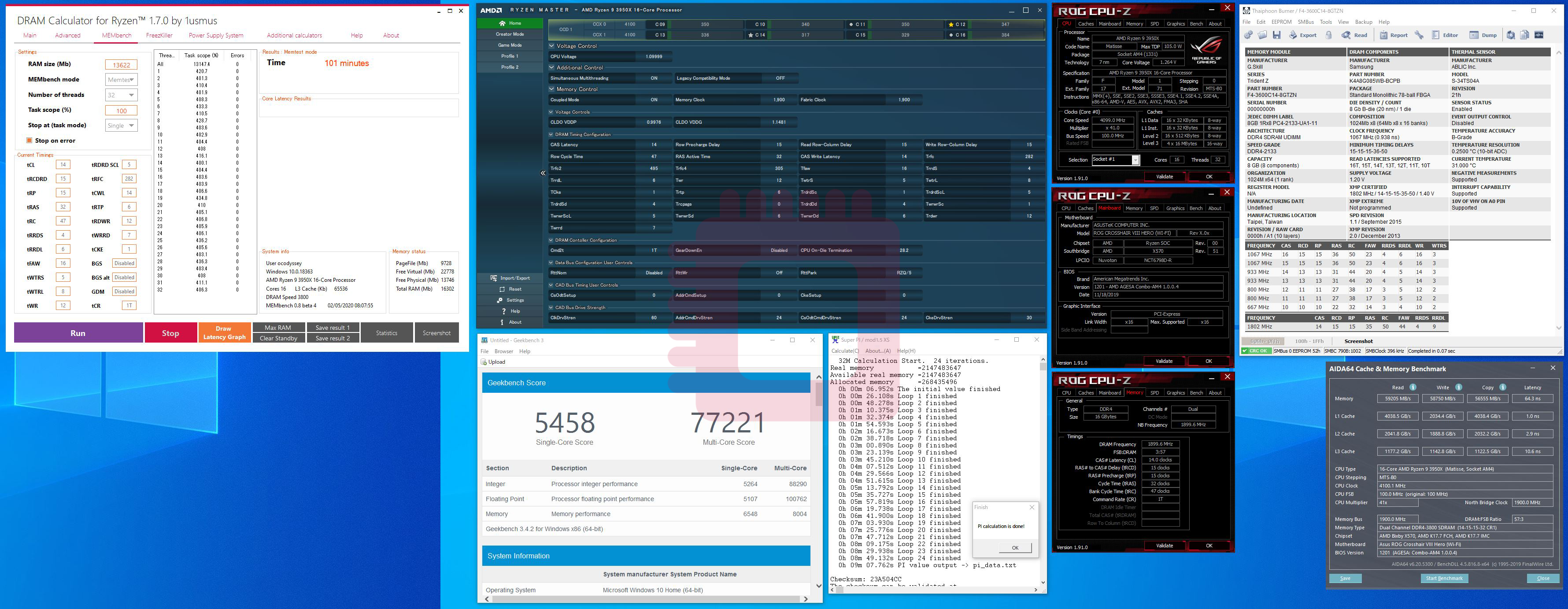
DRAM frequency… 3800 MHz
1st timings: CL 14, tRCD_R 15, tRCD_W 15, tRP 15, tRAS 32
Command Rate: 1T
2nd timings: tRRD, 47; tRRD_S, 4; tRRD_L, 6; tFAW, 16; tWTR_S, 6; tWTR_L, 8; tWR, 12; tRFC, 282; tCWL, 14; tRTP, 6; tCKE, 1
3rd timings: TrdrdScL, 5; TwrwrScL, 5; TwrwrScl, 5; Trdwr, 8; Twrrd, 2; TwrwrSc, 1; TwrwrSd, 6; TwrwrDd, 6; TrdrdSc, 1; TrdrdSd, 4; TrdrdDd, 4
DRAM voltage: 1.48000 V
VTT DDR: 0.74375 V
CPU SoC voltage: 1.08125 V
Rtt: RTT_NOM, Disable; RTT_WR, off; RTT_PARK, RZQ/5
ProcODT: 28.2 Ohm
CAD_Bus Drive Strength: CAD_Bus ClkDrv, 60.0 Ohm; CAD_Bus AddCmdDrv, 24.0 Ohm; CAD_Bus CsOdtDrv, 24.0 Ohm; CAD_Bus CkeDrv, 30.0 Ohm
VDDP Voltage: 0.94500 V


